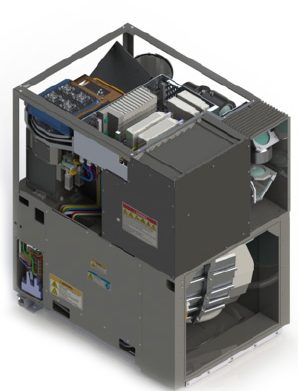
 Development Goals:
- Comprehensive inline inspection of defects
- High sensitivity of up to 0.5 microns at high throughput of 120 Wph
- High stability and low cost-of-ownership due to a “no-moving parts” design
task:
- concept development and construction
- production and assembly support of the prototypes
- CE and Semi certification
- series redirection
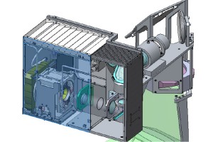 In the scope of the project :
- optimize camera properties with better cooling, EMC protection, and shutter integration
- realization of a camera adjustment concept with a reproducible 3-point support
- mechanical development of the lens and tube lens
- integration of incident lighting
- Development of a filter wheel
- construction of a filter wheel with two separate drives
Here you will find our range of services for your application.
We are happy to support you here in your development & construction.
Do you have any questions? Then please contact us here.
In addition, we are your ISO 9001 certified partner for the production and assembly.